

386 motherboard using the MX83C305/MX83C05 chipset © 199? Unknown
This chipset was designed to integrate the majority of the "AT-compatible" logic onto a very small footprint. Boards utilizing this chipset are characterized by a clean, minimalist design—often featuring very few discrete logic chips outside of the core Macronix set. It was a favorite for small-to-medium volume OEMs who needed a reliable turnkey solution for their 386DX desktop systems.
Chipset Architecture:
MX83C305 (System Controller): Managed CPU interface, memory timing, and bus arbitration.
MX83C05 (Peripheral Logic): Handled the system support functions, including DMA, interrupt control, and timer logic.
CPU Support: Strictly 386DX (up to 33MHz or 40MHz).
Expansion: Designed primarily for the ISA bus. It provides a "standard-issue" 386 experience, emphasizing compatibility over high-performance VLB or PCI features.
Memory: Typically supported up to 16MB or 32MB of RAM, often using 30-pin SIMM banks.
Cache: Supports standard L2 cache (usually 64KB or 128KB in DIP sockets).
The "Macronix" Footprint: Boards using this chipset are often easily identifiable by the lack of complex glue logic. If you see a 386 motherboard that looks surprisingly empty but is fully functional, it is almost certainly a Macronix-based design.
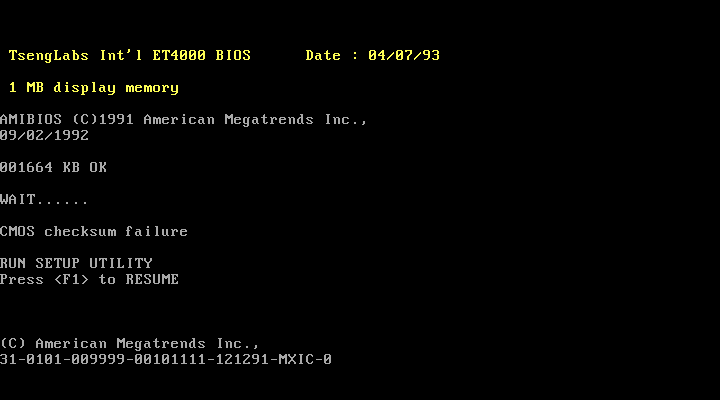
The Battery Problem: Like almost all boards from this period, these systems used the dreaded Varta barrel battery. Because the MX chipset is quite compact, these batteries were often placed right next to the Northbridge/Southbridge chips, meaning that if you are refurbishing one of these, you are highly likely to find trace damage on the high-speed data lines near the MX83C305.